Samsung recently hosted its annual tech day where it had impressive announcements to make. The company is already working on next-generation memory standards for GPUs and RAM, namely the DDR6, GDDR6+, GDDR7 & HBM3.
German publication Computerbase managed to get a hold of the information Samsung shared during its announcement. DDR5 memory is still new to the market, but Samsung is already working on the next generation DDR6.
DDR6
According to the specifications shared by Computerbase, DDR6 should bring double the transfer speeds over DDR5, and quadruple over the DDR4 memory standard. The expected speeds are suggested to be over 12,800 Mbps and more than 17,000 Mbps for overclocked hardware. However, Samsung is teasing even more potential speeds for the future.
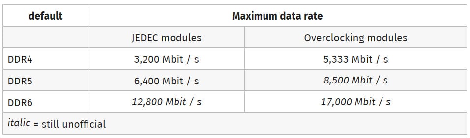
Some manufacturers have teased up to 12,000 Mbps peak speeds for DDR5 memory, so we can expect DDR6 to cross the 20,000 Mbps mark in its most refined state in the future. Further, the DDR6 memory will bring 16-bit memory channels for a total of 64 memory banks.
GDDR6+ and GDDR7
Samsung has also talked about GDDR6+, the GPU memory standard that will replace the current GDDR6. It is more of a refinement over the previous generation rather than just upping bandwidth speeds as always. It will be a part of the next-generation GPUs and will boast up to 24 Gbps speeds. This will allow 256 bit GPUs to reach up to 768 GB/s bandwidth and 320/352/384 bit GPUs up to reach 1TB/s.
As for the GDDR7 roadmap, Samsung is expected to bring 32 Gbps transfer speeds along with a real-time error protection technology. 256 bit GPUs will be able to hit 1TB/s peak bandwidth while a 384 bit and 512-bit system will reach 1.5TB/s and 2TB/s respectively. These are outstanding gains for the GDDR standard.
| Feature | GDDR5 | GDDR5X | GDDR6 | GDDR6X | GDDR6+ | GDDR7 |
|---|---|---|---|---|---|---|
| Density | From 512Mb to 8Gb | 8Gb | 8Gb, 16Gb | 8Gb, 16Gb | 8Gb, 16Gb | 8Gb, 16Gb, 32Gb? |
| VDD and VDDQ | Either 1.5V or 1.35V | 1.35V | Either 1.35V or 1.25V | Either 1.35V or 1.25V | TBD | TBD |
| VPP | N/A | 1.8V | 1.8V | 1.8V | 1.8V | TBD |
| Data rates | Up to 8 Gb/s | Up to 12Gb/s | Up to 16 Gb/s | 19 Gb/s, 21 Gb/s, >21 Gb/s |
24 Gb/s | 32 Gb/s |
| Package | BGA-170 14mm x 12mm 0.8mm ball pitch |
BGA-190 14mm x 12mm 0.65mm ball pitch |
BGA-180 14mm x 12mm 0.75mm ball pitch |
BGA-180 14mm x 12mm 0.75mm ball pitch |
BGA-180 14mm x 12mm 0.75mm ball pitch? |
TBD |
| I/O width | x32/x16 | x32/x16 | 2 ch x16/x8 | 2 ch x16/x8 | 2 ch x16/x8 | TBD |
HMB3
Samsung has also confirmed plans for its next-generation HBM3 memory in Q2 2022, which will power future HPC and data center GPUs/CPUs. SK Hynix has already showcased its new memory modules based on HMB3 with stunning speeds and capacities.
| DRAM | HBM1 | HBM2 | HBM2e | HBM3 |
|---|---|---|---|---|
| I/O (Bus Interface) | 1024 | 1024 | 1024 | 1024 |
| Prefetch (I/O) | 2 | 2 | 2 | 2 |
| Maximum Bandwidth | 128 GB/s | 256 GB/s | 460.8 GB/s | 819.2 GB/s |
| DRAM ICs Per Stack | 4 | 8 | 8 | 12 |
| Maximum Capacity | 4 GB | 8 GB | 16 GB | 24 GB |
| tRC | 48ns | 45ns | 45ns | TBA |
| tCCD | 2ns (=1tCK) | 2ns (=1tCK) | 2ns (=1tCK) | TBA |
| VPP | External VPP | External VPP | External VPP | External VPP |
| VDD | 1.2V | 1.2V | 1.2V | TBA |
| Command Input | Dual Command | Dual Command | Dual Command | Dual Command |
The tables are taken from Wccftech.
Stay Connected with ProPakistani
Get the latest tech news, telecom insights, and product launches wherever you prefer.
Add ProPakistani to Preferred Sources and see more of our stories in Google Search and Top Stories.