Researchers at the Samsung Advanced Institute of Technology (SAIT) have been working on enhancing the compatibility of graphene with silicon-based semiconductor processes for a long time.
Finally, in collaboration with the Ulsan National Institute of Science and Technology (UNIST) and the University of Cambridge, SAIT has unveiled the discovery of a new material called amorphous boron nitride (a-BN) that possesses the power to change the development and commercialization of semiconductors.
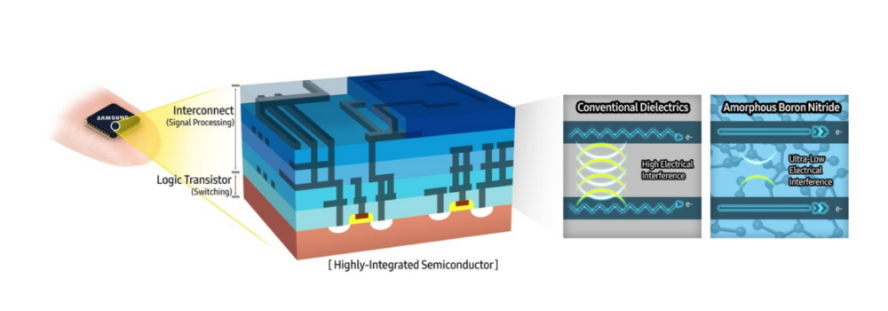
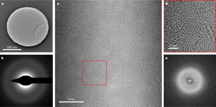
The material is a derivative of white graphene that includes both Boron and Nitrogen atoms arranged in a hexagonal structure. However, a-BN has a molecular structure that makes it uniquely distinctive from white graphene, giving it the ideal properties for creating the next generation of semiconductors.
According to Samsung:
Amorphous boron nitride has a best-in-class ultra-low dielectric constant of 1.78 with strong electrical and mechanical properties and can be used as an interconnect isolation material to minimize electrical interference.
For the uninitiated, the lower the dielectric constant, the higher are the material’s electrical conduction properties. Hence, a-BN’s dielectric constant promises properties like reduced signal delay, high-temperature endurance, and flame retardancy.
As per Samsung’s report, the new material is expected to be widely applied to semiconductors such as DRAM and NAND solutions, and especially in next-generation memory solutions for large-scale servers.